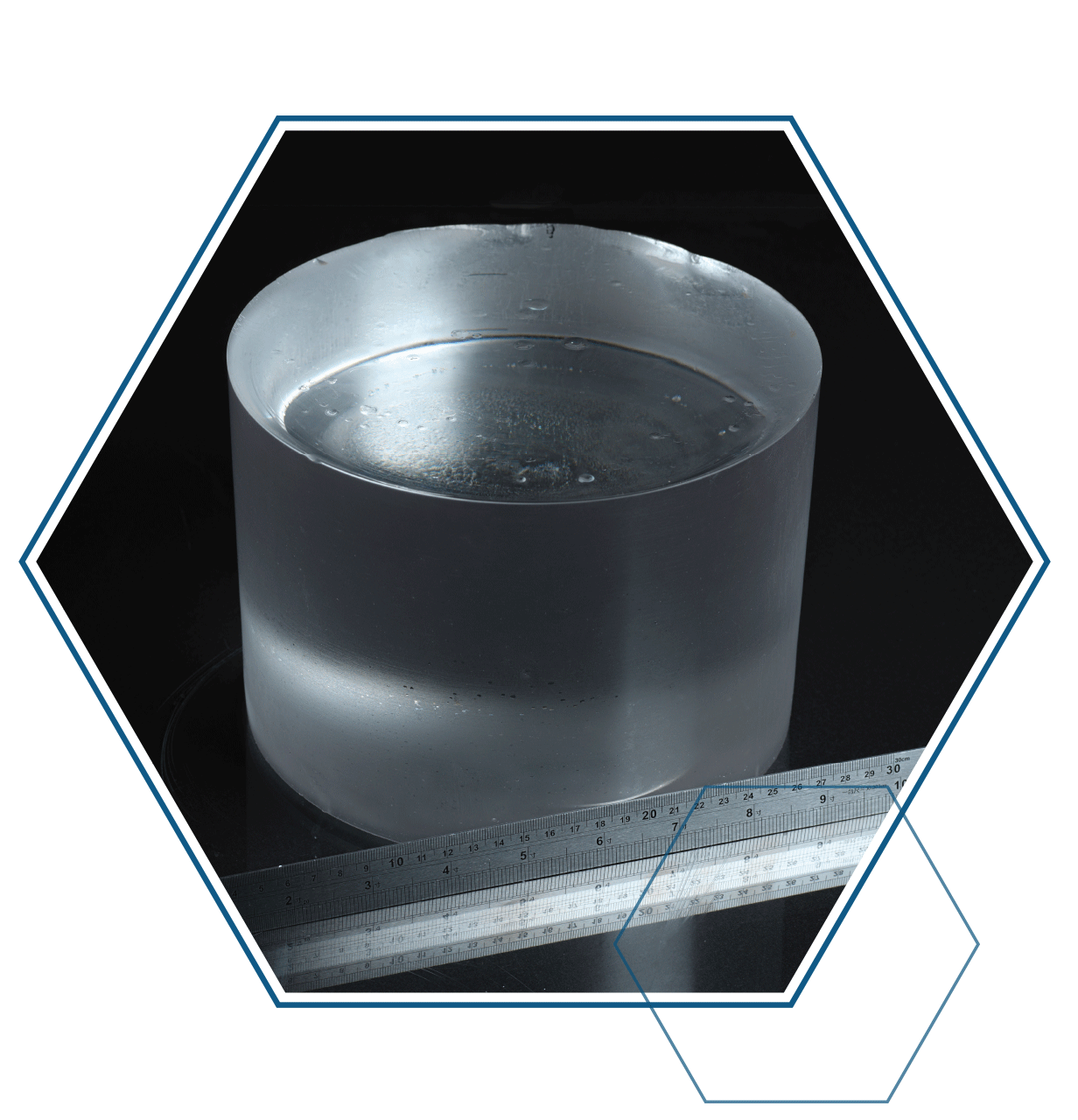
NEWS
FAMETEC is part of ICSCRM 2025
Visit our Advanced Materials experts at ICSCRM 2025 from September 14th to 19th, 2025 in Busan, Korea. You will find us at booth #67.
NEWS
FAMETEC is part of CSI 2025
Visit us at CSI 2025 and get to know our experts of FAMETEC and EEMCO. We are looking forward to meeting you there.
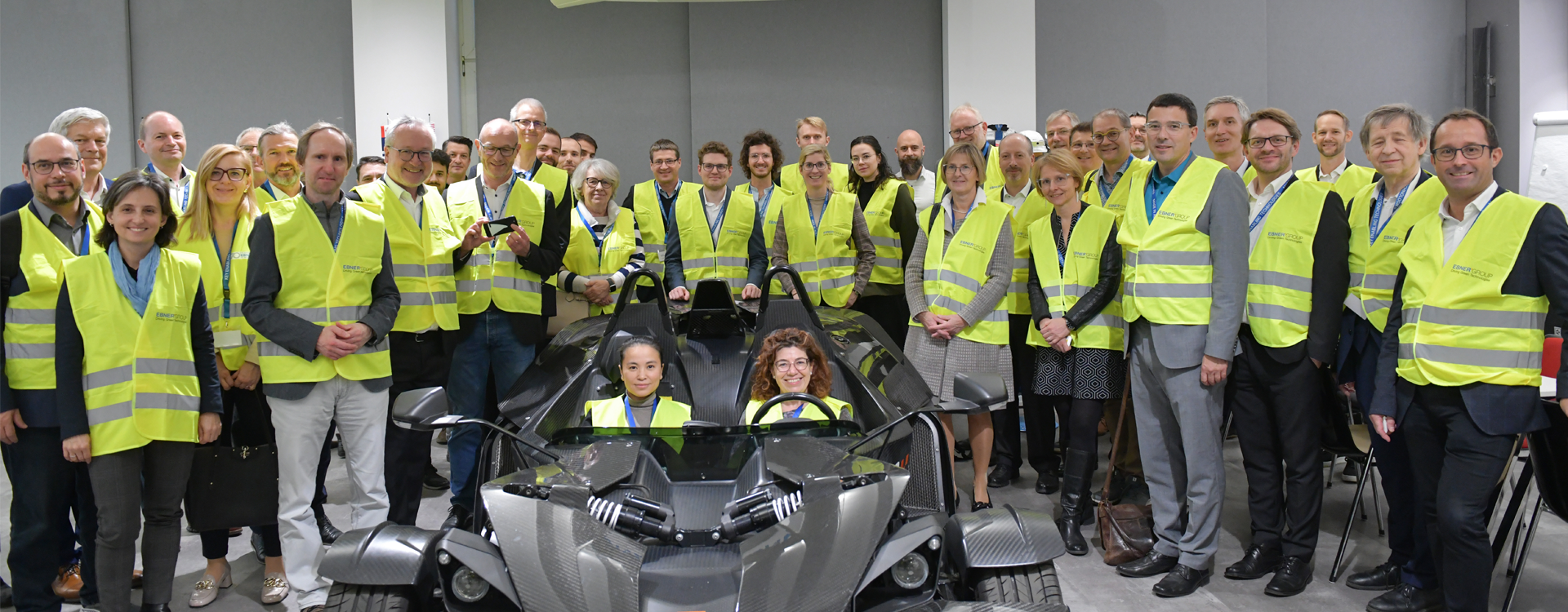
NEWS
Annual ESBS Meeting at EBNER Leonding
On November 7th, we proudly hosted the 2024 annual meeting of ESBS Austria (Electronics and Software Based Systems Austria) at EBNER Leonding.